The TI LaunchPad uses the TM4C123GH6PM microcontroller, which has 256K bytes (256KB) of on-chip Flash memory for code, 32KB of on-chip SRAM for data, and a large number of on-chip peripherals.
The ARM Cortex-M4 has 4GB (Giga bytes) of memory space. It uses memory mapped I/O, which means that the I/O peripheral ports are mapped into the 4GB memory space.
| Allocated size | Allocated address | |
| Flash | 256 KB | 0x0000.0000 to 0x0003.FFFF |
| SRAM | 32 KB | 0x2000.0000 to 0x2000.7FFF |
| I/O | All the peripherals | 0x4000.0000 to 0x400F.FFFF |
2.1 GPIO
The General Purpose I/O ports (GPIO) on TM4C123GXL LaunchPad are designated to port A to port F. The address range assigned to each GPIO port is shown as follows:
- Port A: 0x4000.4000 to 0x4000.4FFF
- Port B: 0x4000.5000 to 0x4000.5FFF
- Port C: 0x4000.6000 to 0x4000.6FFF
- Port D: 0x4000.7000 to 0x4000.7FFF
- Port E: 0x4002.4000 to 0x4002.4FFF
- Port F: 0x4002.5000 to 0x4002.5FFF
It is worth mentioning that 4K bytes of memory space is assigned to each of the GPIO. The reason is that each GPIO has a large number of special function registers associated with it, and furthermore GPIO Data Register supports bit-specific addressing, which allows collective access to 1 to 8 bits in a data port.
To initialize an I/O port for general use seven steps need to be performed. Some registers are needed for the configuration. Figure 2.1 provides an overlook about these registers and their addresses.
1) Activate the clock for the port in the Run Mode Clock Gating Control Register 2 (RCGC2).
2) Unlock the port. This step is only needed for pins PC3-0, PD7 and PF0 on TM4C123GXL LaunchPad.
3) Disable the analog function of the pin in the Analog Mode Select register (AMSEL), because we want to use the pin for digital I/O. If this pin is connected to the ADC or analog comparator, its corresponding bit in AMSEL must be set as 1. In our case, this pin is used as digital I/O, so its corresponding bit must be set as 0.
4) Clear bits in the port control register (PCTL) to select regular digital function. Each GPIO pin needs four bits in its corresponding PCTL register. Not every pin can be configured to every alternative function. Figure 2.2 show which pin can be used as what kinds of alternate functions.
5) Set its direction register (DIR). A DIR bit of 0 means input, and 1 means output.
6) Clear bits in the alternate Function Select register (AFSEL).
7) Enable digital port in the Digital Enable register (DEN).
Please note that we need to add a short delay between activating the clock and setting the port registers. As you can see in Figure 2.1, PC0-PC3 is used for JTAG connections to the debugger on the LaunchPad. So we’d better do not use these pins normally.

Now let’s have a look at GPIO Data Register in detail. The GPIO Data Register is located at the offset address of 0x000 from the base address of its port. As we mentioned before, the data register supports bit-specific addressing. In order to write to this register, the corresponding bits in the mask, resulting from the address bus bits[9:2], must be set. Otherwise, the bit values remain unchanged by the write.

For example, writing to address 0x40004038 means that bits 1, 2 and 3 of port A must be changed, since the base address of port A is 0x40004000. The explanation is shown in below.

The following table help you calculate offset address for the bits of a port, to which you want to access.
| If we want to access bit | Offset Constanct |
| 7 | 0x200 |
| 6 | 0x100 |
| 5 | 0x080 |
| 4 | 0x040 |
| 3 | 0x020 |
| 2 | 0x010 |
| 1 | 0x008 |
| 0 | 0x004 |
If we we want to read and write all 8 bits of a port, it means that we need to sum all these 8 offset constants, which makes the offset address of 0x3FC (001111111100 in binary).
2.2 Negativ/Positive Logic Switch Interface
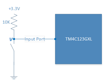
The circuit on Figure 2.3 shows a mechanical switch with a 10K Ohm pull-up resistor attached to the other side. When the switch is not pressed, the pull-up resistor will create a +3.3V at point V. When the switch is pressed, the voltage at point V will be very near to zero. Because the resistance of this switch is quite small comparing to the pull-up resistor. We connect this circuit to an input pin of our LaunchPad. Then we make a program, which can determine whether the switch is pressed or not, by reading the input port. If the switch is not pressed, the software will get a one. If the switch is pressed, it will read a zero. This kind of circuit is called negative logic, because in the active state, when switch is pressed, has a lower voltage.
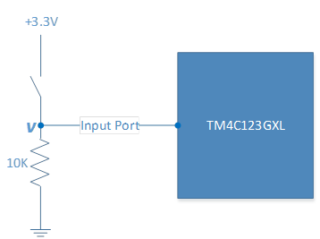
Figure 2.4 shows a positive logic switch interface. Because in the active state, when the switch is pressed, a positive one will be read by the microcontroller, and when the switch is not pressed, a zero will be read.
2.3 GPIO Demo
Below is a list of the components you will need:
- 10K Ohm resistor
- 470 Ohm resistor
- TM4C123GXL LaunchPad
- B3F tactile switch and one LED diode
- One breadboard and some jumper wires
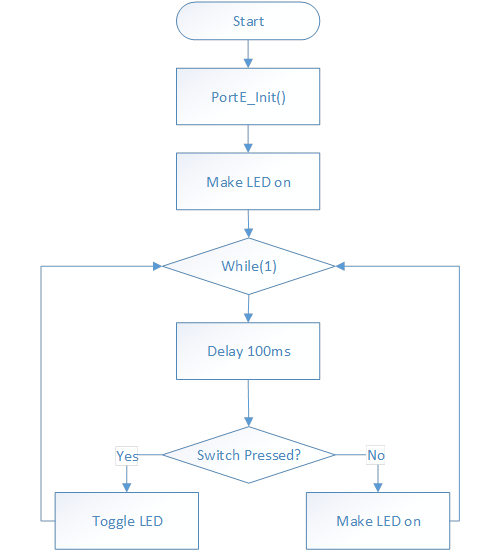
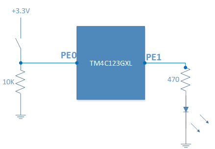
Figure 2.5 shows how this circuit is connected. The following are the source code and its flow chart.
/*
* GPIO Demo
*/
// 1) Make PE1 an output and PE0 an input
// 2) Make LED on initially
// 3) Delay about 100ms
// 4) If the switch is pressed, then toggle LED. Otherwise make LED on
// 5) Repeat 3),4)
#define SYSCTL_RCGC2_R          (*((volatile unsigned long *)0x400FE108))
#define GPIO_PORTE_DATA_R 	    (*((volatile unsigned long *)0x400243FC))
#define GPIO_PORTE_AMSEL_R      (*((volatile unsigned long *)0x40024528))
#define GPIO_PORTE_PCTL_R       (*((volatile unsigned long *)0x4002452C))
#define GPIO_PORTE_DIR_R        (*((volatile unsigned long *)0x40024400))
#define GPIO_PORTE_AFSEL_R      (*((volatile unsigned long *)0x40024420))
#define GPIO_PORTE_DEN_R        (*((volatile unsigned long *)0x4002451C))
#define PE0                     (*((volatile unsigned long *)0x40024004))

void PortE_Init(void) {
  volatile unsigned long delay;
  // 1) activate clock for Port E
  SYSCTL_RCGC2_R |= 0x00000010;
  // allow time for clock to start
  delay = SYSCTL_RCGC2_R;
  // 2) disable analog on PE
  GPIO_PORTE_AMSEL_R &= ~0x03;
  // 3) PCTL GPIO on PE1-0
  GPIO_PORTE_PCTL_R &= ~0x000000FF;
  // 4) PE0 in, PE1 out (1: Output; 0: Input)
  GPIO_PORTE_DIR_R |= 0x02;
  GPIO_PORTE_DIR_R &= ~0x01;
  // 5) disable alternate function on PE1-0
  GPIO_PORTE_AFSEL_R &= ~0x03;
  // 6) enable digital I/O on PE1-0
  GPIO_PORTE_DEN_R |= 0x03;
}

// TM4C1234GXL default bus clock (16MHz)
// Each inner loop needs 6 cycles
void Delay100ms(unsigned long time) {
  unsigned long i;
  while(time > 0) {
    i = 266667;  // This number means 100ms
    while(i > 0) {
      i = i - 1;
    }
    time = time - 1; // Decrements every 100 ms
  }
}

int main(void) {
  PortE_Init();
  GPIO_PORTE_DATA_R = 0x02;
  while(1) {
	Delay100ms(1);
    if (PE0) {
	   GPIO_PORTE_DATA_R ^= 0x02;
	}
	else {
	   GPIO_PORTE_DATA_R = 0x02;
	}
  }
}


References
1 Embedded Systems – Shape the World: http://users.ece.utexas.edu/~valvano/Volume1/E-Book/
2 TM4C123GH6PM Microcontroller Data Sheet
| Chapter | Page Number |
| 5.6 System Control Legacy Register Descriptions | 462 |
| 10.5 Register Descriptions | 658 |
The source code of this demo and some documents can be found: https://github.com/jiehou/TM4C123GXL


Leave a comment